USB Type-C/PD Brief Introduction and Analysis
Abstract
The USB specification has evolved from USB1.0 to USB4 over time with the different types of plugs and receptacles, such as Type-A, Type-A SuperSpeed, Mini-B, Micro-B and more. So far, there aren’t any universal connectors for all products. Industry standardization around USB Type-C means a single cable can be shared among different devices from various manufacturers, thus reducing multiple purchases and greatly bringing convenience.
USB Type-C is the latest USB_IF standard for USB 2.0/3.2/4 and DisplayPort. Data, video and power transmission interfaces can be implemented with just one Type-C cable. For the power transmission, it can even support from Type-C max power 15W (5V/3A) to 100W (20V/5A) PD (Power Delivery) where the power flow can be bi-directional.
As a result, nowadays the USB Type-C standard is widely implemented in many consumer electronics such as cell phones, tablets, travel adaptors, monitors, laptops and more. USB Type-C ports contains the conventional pins of Type-A/B like USB data lines DPDM and VBUS. It also adds CC pins to complete normal Type-C functions and PD signals for higher power or for fulfilling the display signal communication on TX/RX and SBU pins. As expected, USB Type-C has gradually become an ubiquitous universal charging standard.
1. System Overview
USB Type-C re-defines the general connector types of receptacles, plugs and cables. It minimizes the connector size and enhances the ease of use by being plug-able in either upside-up or upside-down directions. USB Type-C devices provide multiple functions interfaces such as power supply, data, display, etc. All functions are integrated into one hardware interface, including :
(1). VBUS supplies power to the USB devices. The max power is 100W for USB PD 3.0 specification.
(2). CC is used in USB PD functional communication with power management.
(3). VCONN provides power to E-marker cable and VCONN powered accessories.
(4). SBU is the auxiliary channel for two-way transmission of display and data signals.
(5). DP/DM provides data transmission USB2.0 (480Mbps) data and battery charge detection.
(6). SSTX/RX pair is used for high-speed data or display data in up to 40Gbps speed.
(7). The IEC61000-4-2 ESD standard defines contact discharge protections for each pin on the Type-C port indifferent application platforms, such as PC, monitors, NB, and mobile phones, which will be explained in the following chapter.
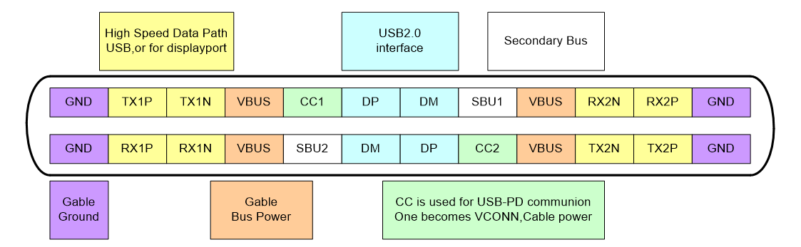
Figure 1. Type-C Pin Assignment
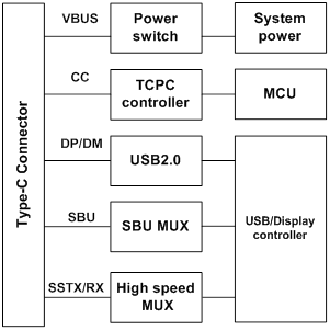
Figure 2. USB Type-C System Blocks
2. Power Application on Type-C Platforms
2-1. Type-C Functional Model for System
Type-C state can be presented as Dual-Role Power Port (DRP) where the port can be assigned as a source role or a sink role (see Figure 3). In the DRP system, Rp is used to behave as source and Rd is used to be as sink. DRP will present Rp and Rd simultaneously to represent as both source and sink implementation. It can supply power or consume power over VBUS.
When Type-C state is presented as source port only (see Figure 4), the port is able to supply power over VBUS and must assert a pull-up resistor (Rp) resistor on the configuration channel (CC) pins.
When Type-C state is presented as sink port only (see Figure 5), the port is able to consume power over VBUS and must assert a pull-down resistor (Rd) on the CC pins.
According to product characteristics, the behaviors on CC and VBUS can be seen in the Table 1. As a result, when an attach event happens, there will be a connection between a source device and a sink device. The source Rp is connected to sink Rd on CC pins and VBUS direction is from source to sink.
Figure 3. DRP Functional Model for CC1 and CC2
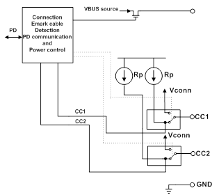
Figure 4. Source only Functional Model for CC1 and CC2
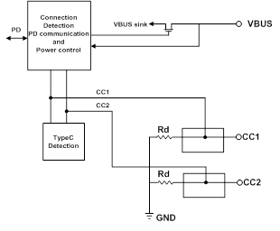
Figure 5. Sink Only Functional Model for CC1 and CC2
Table 1. Comparisons between DRP/Source only/Sink Only
|
DRP
|
Source Only
|
Sink Only
|
|
CC Behavior
|
Rp/Rd toggle
when CC is unattached
|
Present Rp only
when CC is unattached
|
Present Rd only
when CC is unattached
|
|
VBUS Power Flow
|
1. Source VBUS when CC is attached to Rd
2. VBUS Sink to device when CC is attached to Rp
|
Source VBUS
when CC is attached to Rd
|
VBUS Sink to device
when CC is attached toRp
|
|
Product Example
|
Cell phone/notebook/power bank/ Docking/HUB
|
PC/Monitor/ Wall Adapters/ Automotive
|
Monitor/Thumb drive/IOT/WIFI AP/ Drones/Printers/ camcorders/cameras/Toys
|
2-2. Power System Design on Platform
There are some differences between the system design architecture and the Type-C system.
For example, notebooks are DRP systems. VBUS is on the notebook platform. Because notebook batteries are usually 2 to 4 cells, the VBUS design usually operates in the input range of 4.5V to 20V to charge the notebook system. Reducing power consumption is the main consideration on notebook designs. VBUS output only provides 5V/1.5A and the overall system can have higher tolerance range. The VBUS input voltage is up to 20V. The CC/VCONN/SBU1/SBU2/DP/DM OVP protection will be implemented on the pin design to prevent the port from being inserted diagonally, thus causing the port IC to be damaged. The RT1738A provides CC/SBU channel switch with high-bandwidth, short to VBUS protection and IEC61000-4-2 ESD contact discharge protection.
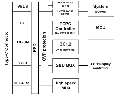
Figure 6. USB Type-C Notebook System Blocks
Monitors are source or sink only systems. VBUS is on the source only platform. The monitor system design is supposed to provide notebook power supply. The power requirement for notebook is 30W~60W. The capacity of VBUS power supply is 5 to 20V/3A or 5A. The monitor system architecture provides external power supply for applications. The system power is not provided by VBUS. The VBUS output voltage is up to 20V. The CC/VCONN/ SBU1/SBU2/DP/DM OVP protection will be implemented on the pin design to prevent the port from being inserted diagonally, thus causing the port IC to be damaged.
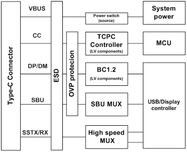
Figure 7. USB Type-C Monitor Source Only System Blocks
The small portable monitors are sink only systems. It consumes less than 7.5W. The main purpose of using a power switch or a MOSFET is to prevent the system damage from abnormal voltage. This is not necessary if preventing system damage is not a concern. However, if the driving voltage is higher than 5V, it is necessary to add a high voltage protection function on the CC/VCONN/DP/DM/SBU1/SBU2 pins.
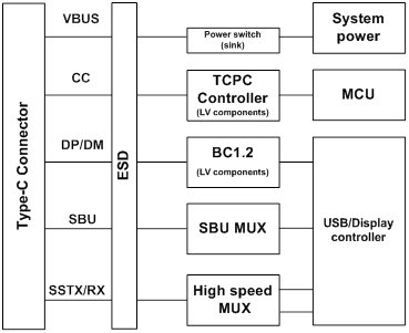
Figure 8. USB Type-C Monitor Sink Only System Blocks
Personal computers are source only systems. VBUS is on the personal computer platform. The power supply of personal computers is only 3.3V/5V/12V/-12V and personal computers consume more than 100W. Personal computers do not need VBUS to provide power and only require the power supply with the capacity of 5V/3A. The VBUS is controlled by a power switch. The maximum voltage of VBUS is 5V. The CC/VCONN/SBU1/SBU2/DP/DM pins usually do not require extra components for OVP protection to reduce cost.
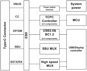
Figure 9. USB Type-C personal computer System blocks
Power system is the main consideration on the Type-C system designs. Designers can change power range based on different system requirements. When VBUS is applied a voltage higher than 5V, the RT1718S provides CC/VCONN/SBU1/SBU2/DP/DM OVP and IEC 61000-4-2 ±8kV protection in addition to USB PD control.
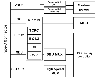
Figure 10. RT1718S USB Type-C System Blocks
The RT1738A is an USB Type-C interface over-voltage protection IC, integrated protection ESDs of IEC61000-4-2 with contact discharge ±8kV on CON_CC1/CON_CC2, D1/D2 and ±6kV on ON_SBU1/CON_SBU2.It is ideal for customers who only need protection functions.
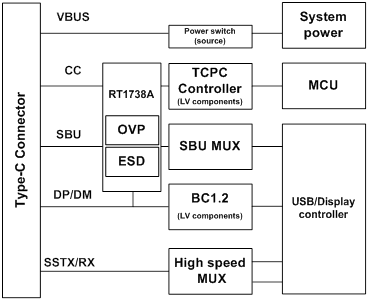
Figure 11. RT1738A USB Type-C System Blocks
For VBUS 5V applications, the RT1715/RT1711P is a cost-effective PD controller solution. The RT1711P has the power path control function, whereas the RT1715 is a PD only controller.
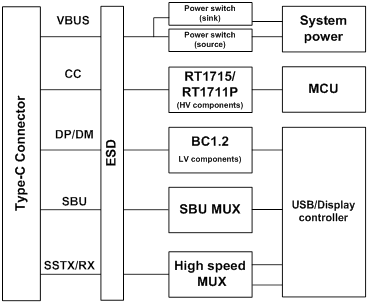
Figure 12. RT1715/RT1711P USB Type-C System Blocks
2-3. Firmware Application of TCPC Controller
In addition to the hardware design, firmware implementation in MCU is also the core control in the Type-C/PD system. Type-C/PD system is based on state machine, protocol and communication between devices, where firmware plays an important role. In the Type-C/PD applications, there are different messages and timers to be programmed. The firmware control is required to meet various requirements in different scenarios Firmware is to solve compliance issues between devices by adjusting some parameters adaptively.
Here is an example of a common timing issue. The OVP switch implementation between two devices, results in the asynchronous timing after OVP switch is off. A time delay should be programmed by firmware to send signals at the right time when VBUS at both sides remains in the same status.
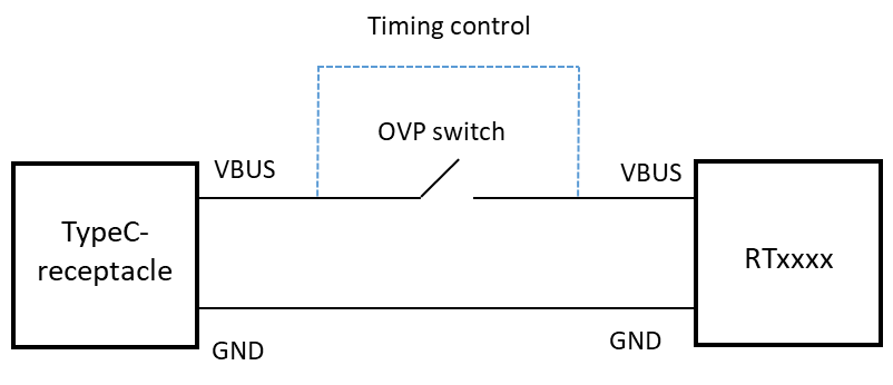
Figure 13. Timing Control with PD Controller
Richtek provides the firmware library of state machine for TCPC series to shorten your product development time. Moreover, we offer the firmware with compliance testing and continually get it updated for new PD specification. The tables below show the resources for different configurations. The TCPC series are recommended for ARM platform. The 8051 platform is not recommended to control multiple ports. Only one MCU is required to control both PD controllers in the TCPC topology. This is more cost-effective than using PD controllers with integrated MCUs. (See Figure 15).
Table 2. ARM M0 and 8051 Platform TCPM Controller Code Size
|
ARM M0 Platform
|
|
Port #
|
Type-C Role
|
Code Size (byte)
|
Ram Size (byte)
|
|
1
|
Dual role
|
22.05k
|
443
|
|
SNK only
|
14.16k
|
369
|
|
SRC only
|
14.14k
|
355
|
|
2
|
Dual role
|
24.99k
|
674
|
|
SNK only
|
16.09k
|
598
|
|
SRC only
|
16.21k
|
578
|
|
8051 Platform
|
|
Port #
|
Type-C Role
|
Code Size (byte)
|
Ram Size (byte)
|
|
1
|
Dual role
|
23.49k
|
663
|
|
SNK only
|
15.57k
|
612
|
|
SRC only
|
16.12k
|
578
|
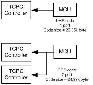
Figure 14. MCU Controller TCPC Controller Code Size
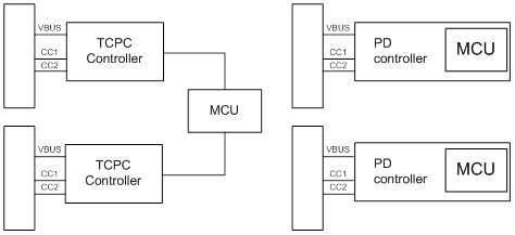
Figure 15. TCPC PD Controller and MCU PD Controller
2-4. Richtek TCPC Controller Function
|
Description
|
RT1715
|
RT1711P
|
RT1718S
|
|
Address Configuration
|
No
|
Address Divider ≥ 4
|
Address Divider ≥ 4
|
|
GPIOs
|
No
|
5
|
3
|
|
Fast Role Swap
|
No
|
No
|
Yes
|
|
VBUS/CC ESD Rating
|
HBM ±2kV
|
HBM ±2kV
|
E-Gun ±8kV
|
|
SBU/DP/DM ESD Rating
|
without pin
|
without pin
|
E-Gun ±8kV
|
|
VBUS Pin AMR Voltage
|
28V
|
28V
|
28V
|
|
CC pin AMR Voltage
|
24V
|
24V
|
24V
|
|
SBU/DP/DM pin AMR Voltage
|
without pin
|
without pin
|
24V
|
|
VBUS ADC
|
No
|
Yes
|
Yes
|
|
CC/SBU/DP/DM ADC
|
No
|
No
|
Yes
|
|
Buck Feedback Controller
|
No
|
Yes
|
No
|
|
Power Path MOS Controller
|
No
|
Yes (N/P MOS)
|
Yes (N/P MOS)
|
|
VBUS Regulator
|
No
|
No
|
Yes
|
|
SBU/DP/DM OVP Switch
|
without pin
|
without pin
|
Yes
|
|
SBU Bandwidth
|
without pin
|
without pin
|
>200MHz
|
|
DP/DM Bandwidth
|
without pin
|
without pin
|
800MHz
|
|
BC1.2 Support
|
without pin
|
without pin
|
Yes
|
|
Package
|
WL-CSP-9B 1.38x1.34 (BSC)
|
WQFN-24L 3.5x3.5
|
WQFN-32L 4x4
|
3. Introduction of Functional Pins
3.1. Power and Ground (VBUS)
In Type-C PD application, the source provides VBUS up to 20V. For safety consideration, it is recommended that the VBUS pin AMR of the Type-C port controller (TCPC) is over 20V even though the VBUS application is only 5V. It is because that the VBUS pin of TCPC must be linked to VBUS pins of the Type-C connector and it is not protected by power switch. For example, some of peripheral devices take only VBUS = 5V. The VBUS pin of TCPC in the peripheral device may be high as 20V due to out of control of power source. The VBUS pin AMR of the RT1715 and RT1711P are up to 24V, and it is up to 28V for the RT1718S.
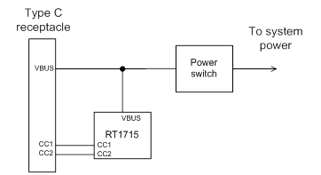
Figure 16. RT1715 VBUS Blocks
The TCPC shall report VBUS status to system manager during attachment and detachment. There are comparators for VBUS present and Vsafe0V detection in the RT1715, RT1711P and RT1718S. Moreover, there is a ADC in the RT1711P and RT1718S, and the variation is ±50mV (2 LSB). It also provides VBUS alarm high/low functions to monitor VBUS, and the setting step of VBUS alarm high/low functions is 25mV.
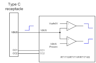
Figure 17. RT1715/RT1711P/RT1718S VBUS Detection Blocks
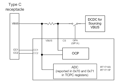
Figure 18. RT1715/RT1711P/RT1718S VBUS ADC Blocks
More advance, there is VBUS over-current protection function (OCP) in the RT1711P and RT1718S. Once VBUS OCP is triggered, the RT1711P and RT1718S turn off the external power path automatically. In the RT1711P, VBUS OCP threshold can be set from 0.5A to 5A with 0.5A per step. In the RT1718S, not only the VBUS OCP threshold can be set from 0.2A to 12.9A with 0.1A per step, but also the de-bounce times can be set from 0ms to 1270ms/6350ms with 10ms/50ms per step. For faster response to VBUS OCP at high VBUS current, there is another comparator for the result of VBUS current sensing in the RT1718S. The VBUS OCP scenario of the RT1718S provides high compliance with high peak current loading sink devices. For example, monitor and notebook are linked through Type-C cable. Monitors provide power to notebooks and get display from notebooks. Notebooks can sink VBUS current with high peak current.
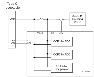
Figure 19. RT1715/RT1711P/RT1718S VBUS OCP Blocks
For better compliance, it is recommended that there is a discharge circuit on VBUS net. There is VBUS discharge function in the RT1718S. It takes 172ms to discharge a 20µF capacitor from 20V to 5V and 232ms to discharge a 20µF capacitor from 20V to 0.4V.
The RT1718S also supports Fast Role Swap function. Especially as an initial sink, the RT1718S controls load switch IC when VBUS falls below the fast role swap VBUS level with fast role swap signal received.
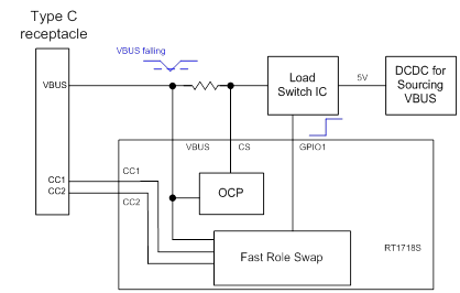
Figure 20. RT1718S Fast Role Swap Blocks
3.2. Configuration
Channel (CC)
In Type-C, there are two configuration channels for attaching and detaching of devices, and the PD communication signal is transmitted through the CC pins. They are used to establish and manage the Source-to-Sink connection. Functionally, the configuration channel is used to serve the following purposes :
- Detect attach of USB ports, e.g. a Source to a Sink.
- Resolve cable orientation and twist connections to establish USB data bus routing.
- Establish data roles between two attached ports.
- Discover and configure VBUS : USB Type-C Current modes or USB Power Delivery Configure VCONN.
- Discover and configure optional Alternate and Accessory modes.
As for the Type-C Plug Flip-ability, USB Type-C plug can be inserted in either right-side-up or upside-down position that CC can judge which side is attached for data communication so that device and host will operate.
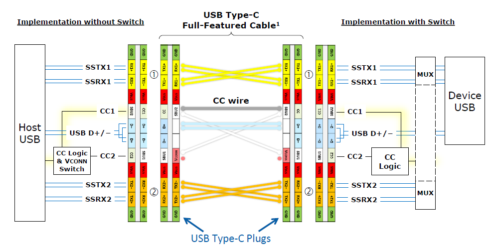
Figure 21. Logical Model for Data Bus Routing across USB Type-C-Based Ports
For Type-C receptacle and plug, it's no longer to differentiate host and device roles based on connector shape like Type-A or Type-B. Both power roles of source and sink can be applied in Type-C connector based on CC pins, and the device can present only source, sink or DRP depending on its capability to wait for connection. For example, the following Figure shows the complete CC models which can present DRP, VCONN supply for E-mark cable and PD communication.
As for the Power Delivery application, the signal transmission is also through CC pins, which is needed to implement with Physical Layer. The RT1715/RT1711P/RT1718S are linked to the Protocol layer controlled by Policy Engine and Device Policy Manager; the whole PD communication system can be built up.
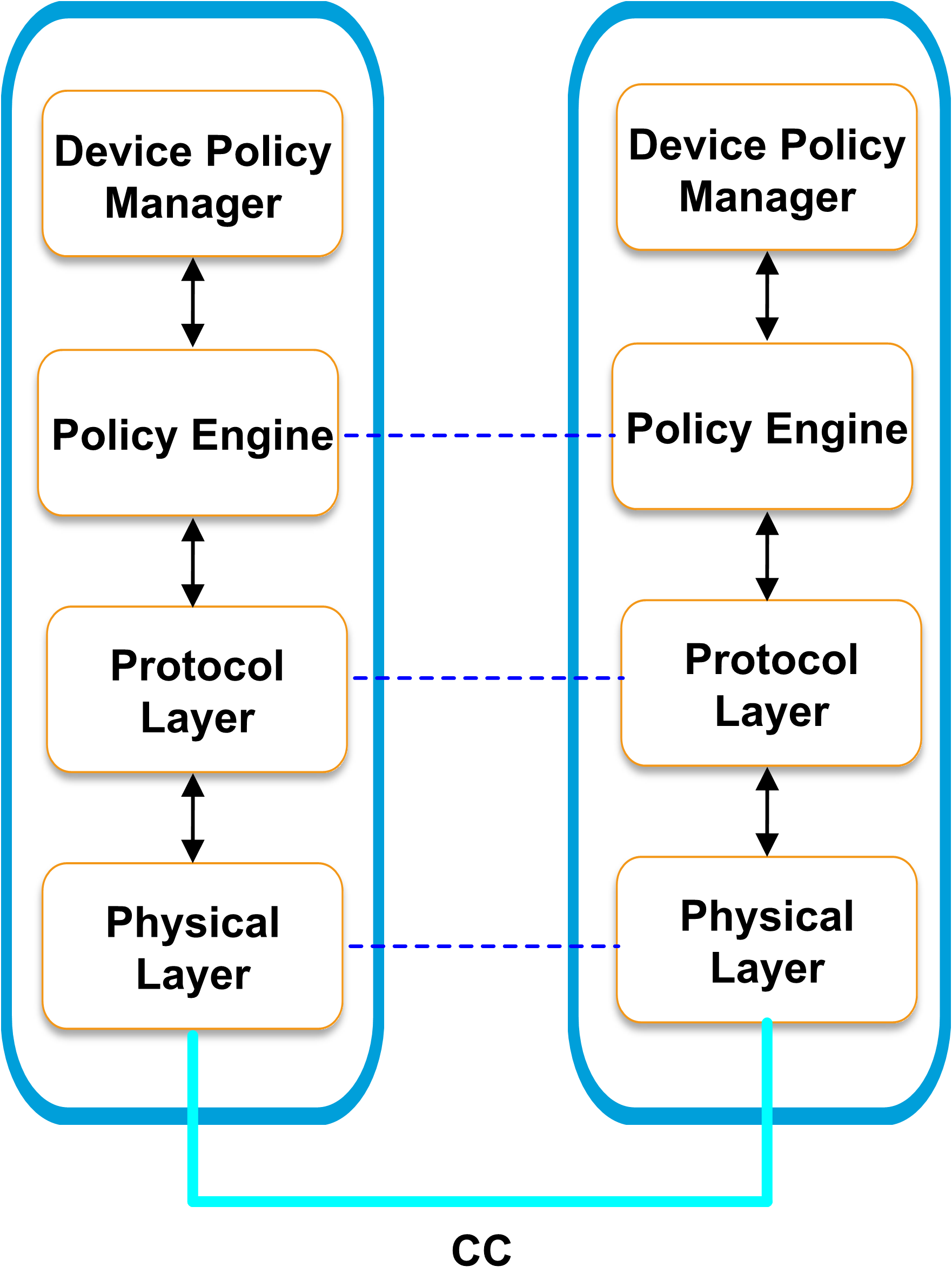
Figure 22. Power Delivery Communications Stack
3.3. PD Communication
In PD communication system, the messages between source, sink devices and e-mark cable is shown in Figure 23. The Start of Packet (SOP) is used as an addressing scheme to identify whether the communications were intended for one of the Port Partners (SOP Communication) or one of the Cable Plugs (SOP’/SOP’’ Communication).
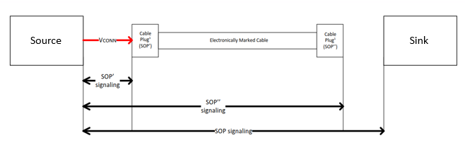
Figure 23. Example of PD Communication with SOP/SOP’/SOP”
The communication mechanism is described in Figure 24. There will be a sender and receiver that the communication is built by which sender initiates a message to the receiver and receiver responds with a message after dealing with the message sent from sender.
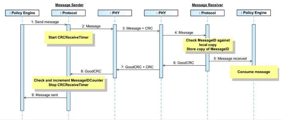
Figure 24. Basic Message Exchange
In Figure25, take a power negotiation between a source, e-mark cable and sink devices which the log message is processed by USB-IF compliance tool Ellysis as an example.
Source sends discover identity message to get cable information and cable responds with its relative message to let source know. Then, source sends its sourcing capability to sink device and sink device requests the voltage and current requirement according to its need.
In short, the communication system can be built up by sending and responding messages which is controlled by the PD communication stack mentioned above.
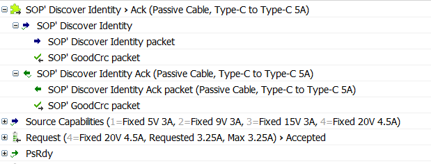
Figure 25. PD Communication Log
3.4. USB 2.0 (DP/DM)
The USB system uses a 2-wire (DP and DM) differential bidirectional system to transfer data. In addition to transferring data, the system is used to power downstream devices and monitor USB data lines (DP and DM) through automatic detection features, and according to the USB battery charging specification (BC1.2) to support the charging system configuration to charge the device.
The BC1.2 specification defines a mechanism that allows USB devices to draw higher current than standard USB: USB2.0 is 500mA, and USB3.0 is 900mA.
Through the mechanism defined in the BC1.2 specification, the device can absorb up to 1.5 A of current. When connected, detect and announce higher current ports through USB2.0 DP and DM lines.
The BC1.2 port types :
Standard Downstream Port (SDP)
SDP is a standard USB port that can support max current up to 500 mA or 900 mA depending on the connection speed. BC1.2 mechanism is not supported.
Charging Downstream Port (CDP)
CDP is a charging USB port with USB data support. A connected device that supports BC1.2 detection can draw up to 1.5 A of current. The CDP advertising device should be able to source voltage 0.5 V to 0.7V on DM for primary detection.
Dedicated Charging Port (DCP)
DCP is a charging only USB port without USB data support. A connected device that supports BC1.2 detection can draw up to 1.5 A of current. The DP and DM lines are shorted through a resistor on DCP.
BC1.2 defines a charging port as a downstream facing USB port that provides power for charging portable equipment.
Table 3. BC1.2 Function
|
Port Type
|
Supports USB 2.0 Communication
|
Maximum Allowable Current Drawn By Portable Equipment (A)
|
|
SDP (USB 2.0)
|
YES
|
0.5
|
|
SDP (USB 3.0)
|
YES
|
0.9
|
|
CDP
|
YES
|
1.5
|
|
DCP
|
NO
|
1.5
|
Some DCP ports support special fast charging and automatic circuit detection functions, which can monitor the voltage of the USB data line. After completing the source and sink handshake, the source port provides a larger charging current to the device.
Such as,
Supports DCP Applying 2.0V on DP and 2.7V on DM & 2.7V on DP and DM
Supports DCP Applying 2.7V on DP and 2V on DM
Supports DCP Applying 1.2V on DP and DM
Table 4. Other Proprietary Protocols for Fast Charging
|
Voltage on DP (V)
|
Voltage on DM (V)
|
Charging Current (A)
|
Comments
|
|
1.2
|
1.2
|
2.1
|
2.1A Chargers
|
|
2
|
2.7
|
1
|
1A Chargers
|
|
2.7
|
2
|
2.1
|
2.1A Chargers
|
|
2.7
|
2.7
|
2.4
|
2.4A Chargers
|
The RT1718S supports USB Charging Port Controller providing USB 2.0 Battery Charging Specification BC1.2 and fast charging mode of mobile devices.
3.5.
Sideband Use (SBU)
The Sideband Use pins (SBU1 and SBU2) are used in Audio Adapter Accessory Mode and Alternate Modes. The Alternate Mode includes USB4, DisplayPort, HDMI, MHL and Thunderbolt over the Type-C interface.
Alternate Modes
The Alternate Mode can be enabled only via a USB PD protocol handshake through structured vendor-defined messages (VDM) to discover, configure, and to enter or exit Alternate Modes. It is highly flexible with multiple high-speed communication lanes and open SBU channels.
The Sideband Channel of a USB4 Port is used to initialize and manage the USB4link between the USB4 ports. The DisplayPort as USB Type-C Alternate Mode AUX signals use SBU1 and SBU2 signal pins, The AUX that is used for link and device management.
Audio Adapter Accessory Mode
The analog audio headsets are supported by multiplexing four analog audio signals onto pins on the USB Type-C connector when in the Audio Adapter Accessory Mode. The four analog audio signals are the same as those used by a traditional 3.5mm headset jack. This makes it possible to use existing analog headsets with a 3.5mm to USB Type-C adapter. Then the RT8980H can implement the audio accessory mode function according to USB Type-C’s requirement, that provide high THDPN performance and high-bandwidth USB and Audio MUX switch.
3.6. SuperSpeed
USB (TX/RX)
The SuperSpeed specification is similar to USB 2.0. The transmission speed of USB3.2 gen2x2 can be up to 20Gbps, and USB4 gen3x2 can be up to 40Gbps. Different communication protocols, such as DisplayPort and Thunderbolts can be switched by PD communication. The transmission speed of SuperSpeed in USB4 is as high as 40Gbps, which is about 80 times faster than USB 2.0 0.48Gbps. It can give a better and faster user experience.
4. Conclusions
The Type-C interface specification allows two-way power supply and data communication capabilities. The focus of the Type-C system design is the optimal design of the power system. If the appropriate design is not used, it will cause an increase in cost and a bad user experience. It is also necessary to increase the design requirements for port protection. In different power system requirements, Richtek provides suitable solutions to customers. It makes PCB circuit design easier and faster for customers.
5. Reference
[1] USB Type-C Specification Release 2.0.pdf
[2] USB_PD_R3_0 V2.0.pdf
[3] USB Developer Days 2016
[4] Product folders : RT1715, RT1711P, RT1718S, RT1738A, RT8980H